In this project, I designed, simulated, and laid out a full 3-bit full adder using 130 nm CMOS technology as part of an advanced VLSI design course. The goal was to work through the entire digital IC design flow, starting from logic design and ending with a verified physical layout.
I implemented the design in Cadence Virtuoso, built the circuit from the transistor level up, verified functionality through simulation, analyzed timing and power performance, and validated the final layout using Calibre LVS. This project was my first glimps into real-world CMOS chip design.
Logic Design and Architecture
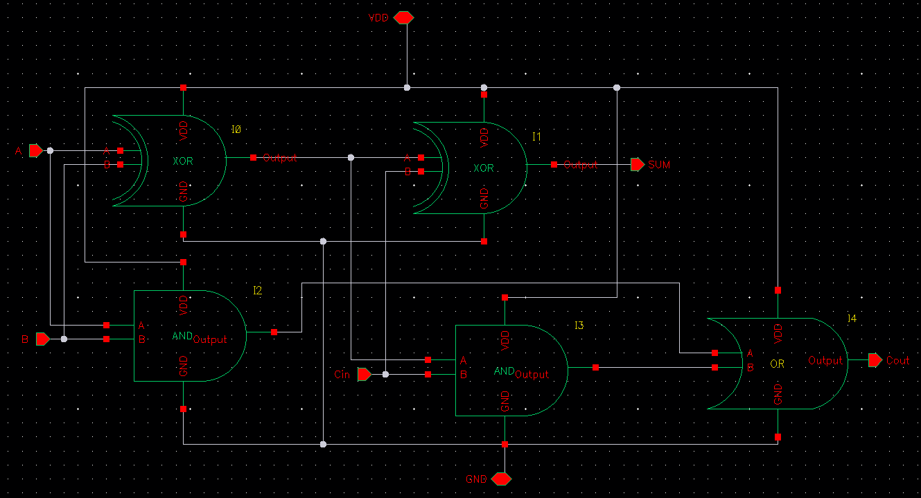
I began by designing a 1-bit full adder, which was the fundamental building block for the full design. I created a truth table to define the relationship between the inputs (A, B, and Cin) and the outputs (Sum and Cout), then simplified the logic using Karnaugh maps.
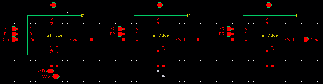
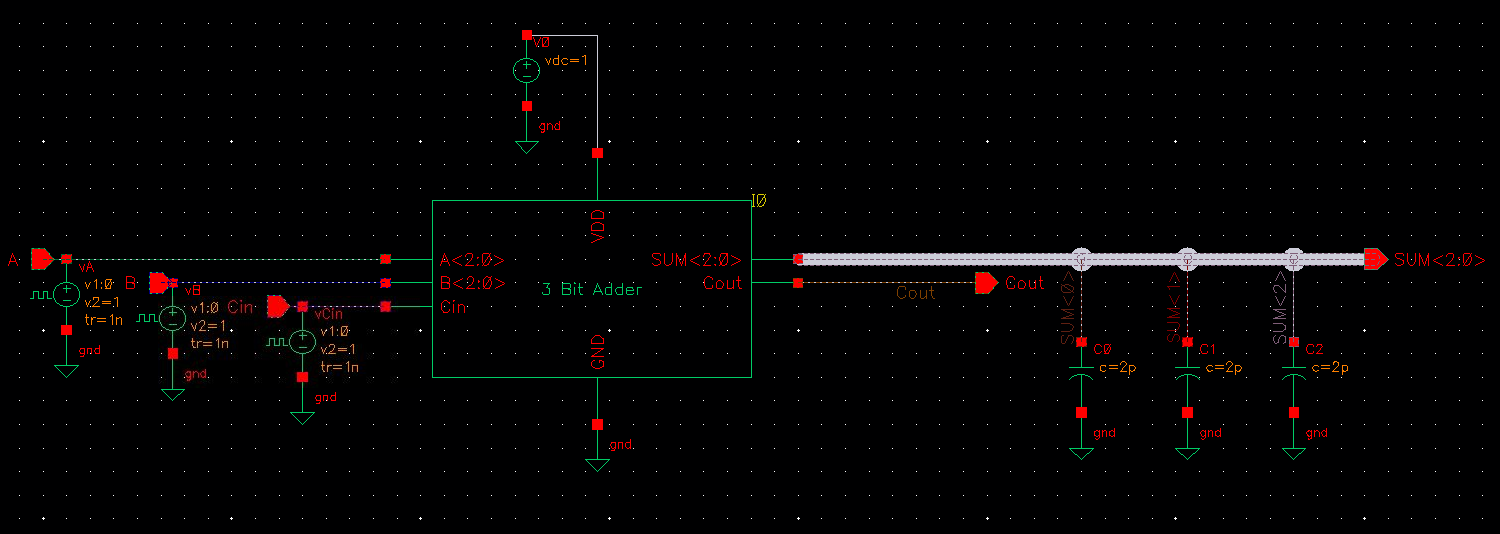
From this, I derived Boolean expressions for both outputs and translated them into a gate-level schematic. To create the final 3-bit adder, I connected three identical full adder blocks in a ripple-carry configuration, where the carry-out of one stage feeds the carry-in of the next.
Transistor-Level Circuit Design
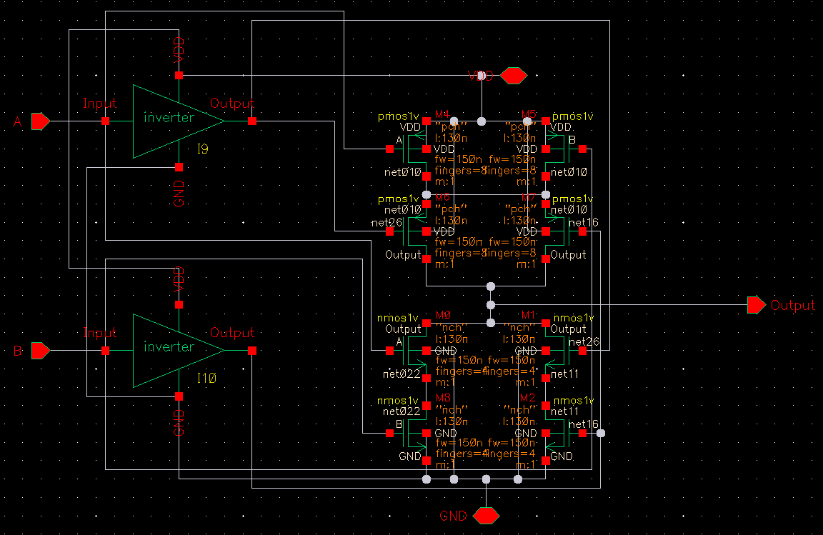
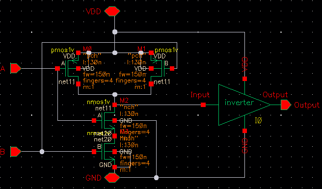
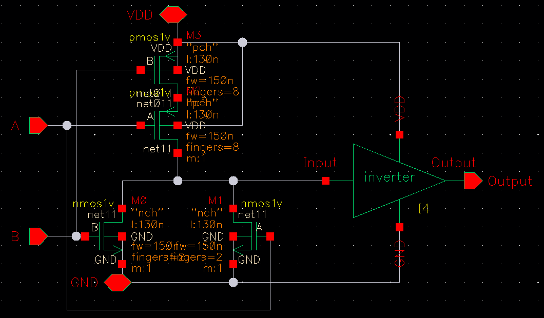
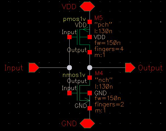
After finalizing the logic, I implemented the design at the transistor level. I first defined a reference inverter to standardize transistor sizing across the design. Using this reference, I built the required logic gates (AND, OR, and XOR) and combined them into a complete full adder cell.
To improve layout consistency and reduce resistance effects, I used fingered transistors with a fixed gate length. Once the full adder cell was complete, I then create the full 3-bit adder schematic.
Testbench and Functional Verification
To verify correct operation, I created a custom testbench that allowed me to easily vary inputs and observe outputs.
I applied timed pulse signals to the input buses so that multiple input combinations were exercised during a single transient simulation. The resulting waveforms confirmed that the adder produced correct sums and carry outputs across all tested cases.
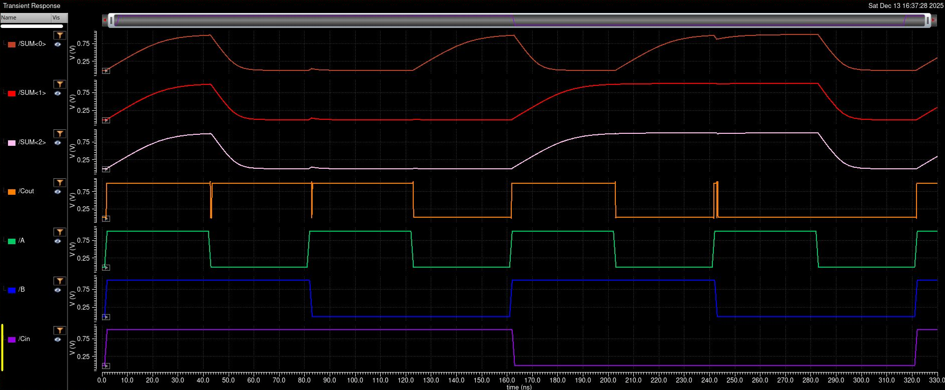
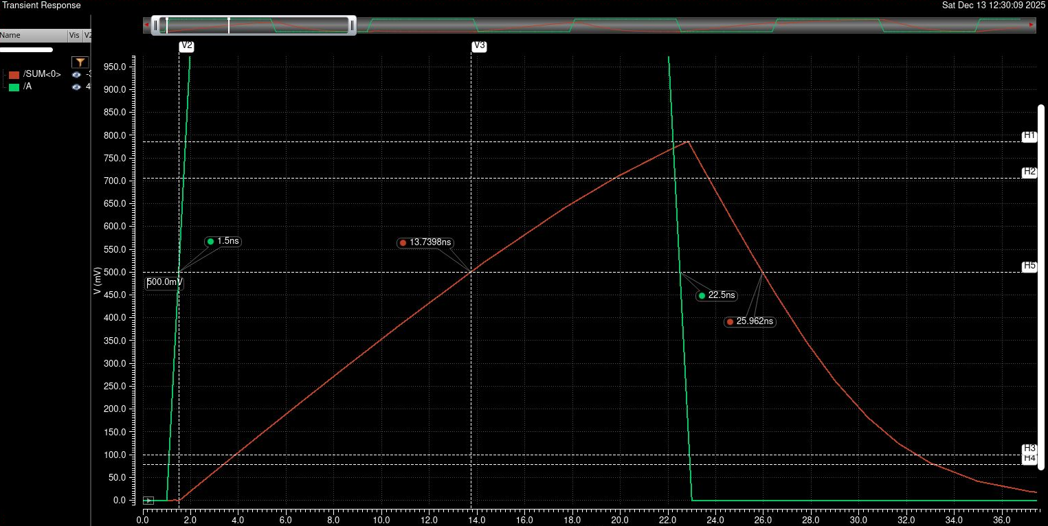
Timing Performance Analysis
Using the simulated waveforms under typical operating conditions, I measured key timing metrics such as rise time, fall time, and propagation delay. This helped me understand how the ripple-carry structure impacts overall performance and where delays accumulate in the circuit.
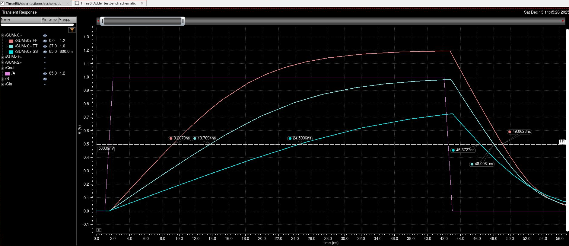
Corner and Robustness Analysis
To evaluate how the design behaves under variation, I ran simulations across slow-slow (SS), typical-typical (TT), and fast-fast (FF) process corners. I adjusted supply voltage and temperature accordingly and compared the resulting delays.
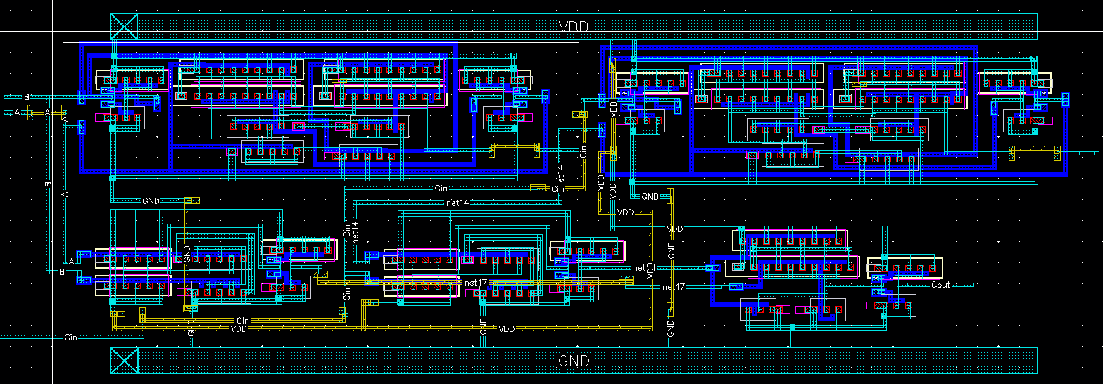
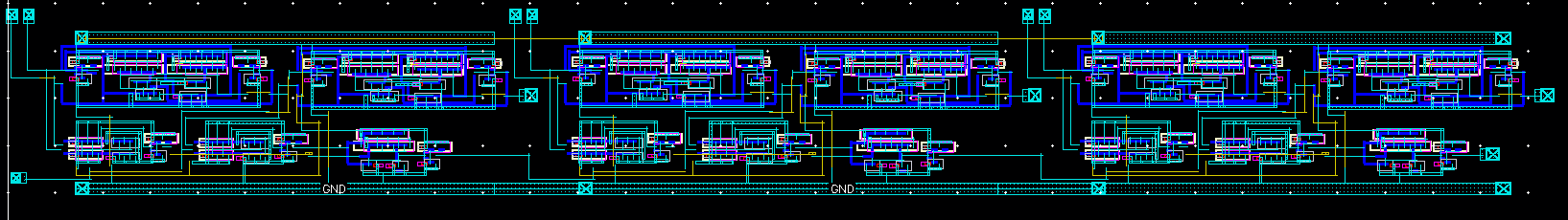
Physical Floorplanned Layout and Verification
Finally, I designed the physical layouts for each logic cell and for the complete 3-bit adder. I followed a bottom-up approach, starting with basic gates and building up to the full system.
All layouts successfully passed Calibre LVS, confirming that the physical implementation matched the schematic design. This step validated that the circuit was correctly implemented at both the electrical and physical levels.