Low Noise Amplifier Design
In this project, completed over several laboratory sessions, I designed, simulated, and analyzed a low-noise amplifier circuit that I built in AWR Microwave Office. This low-noise amplifier was built in stages with analysis done throughout each stage where I would apply concepts such as biasing and impedance matching.
Across the labs, I incrementally built up the knowledge needed to design the complete RF amplifier, starting from basic transistor characterization and ending with a fully tuned, high-gain cascode LNA.
Transistor Characterization and Biasing
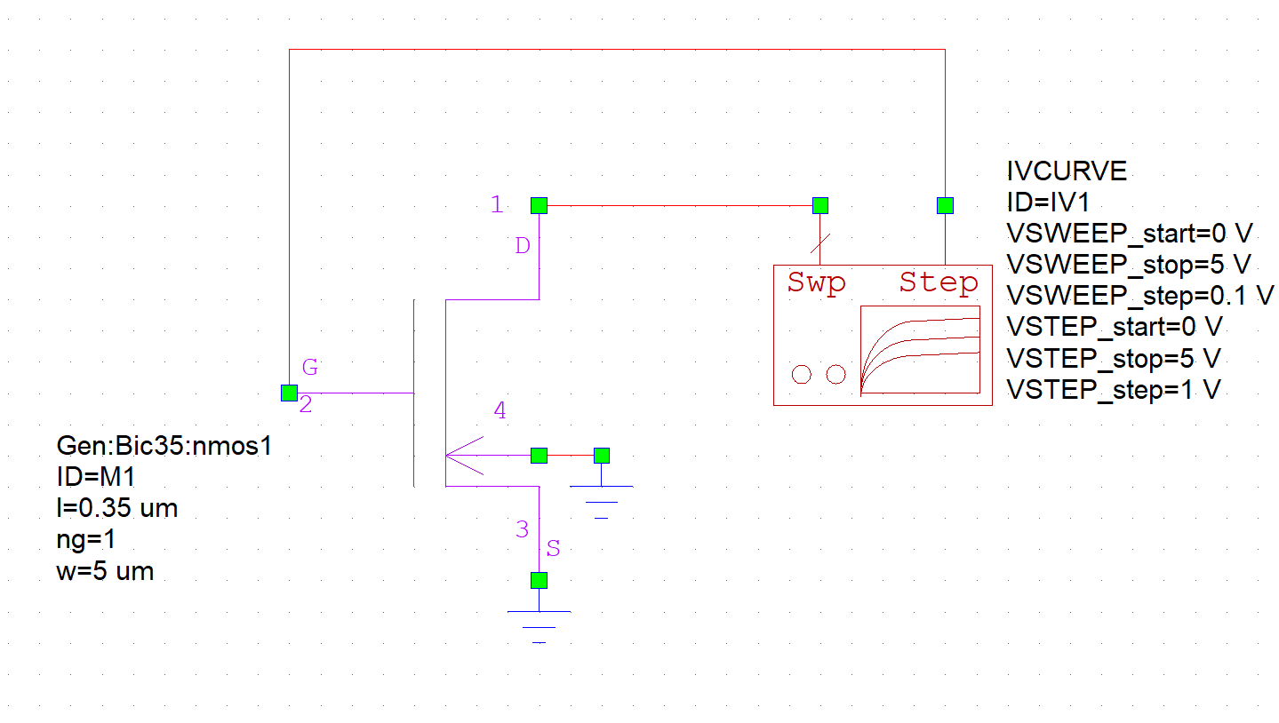
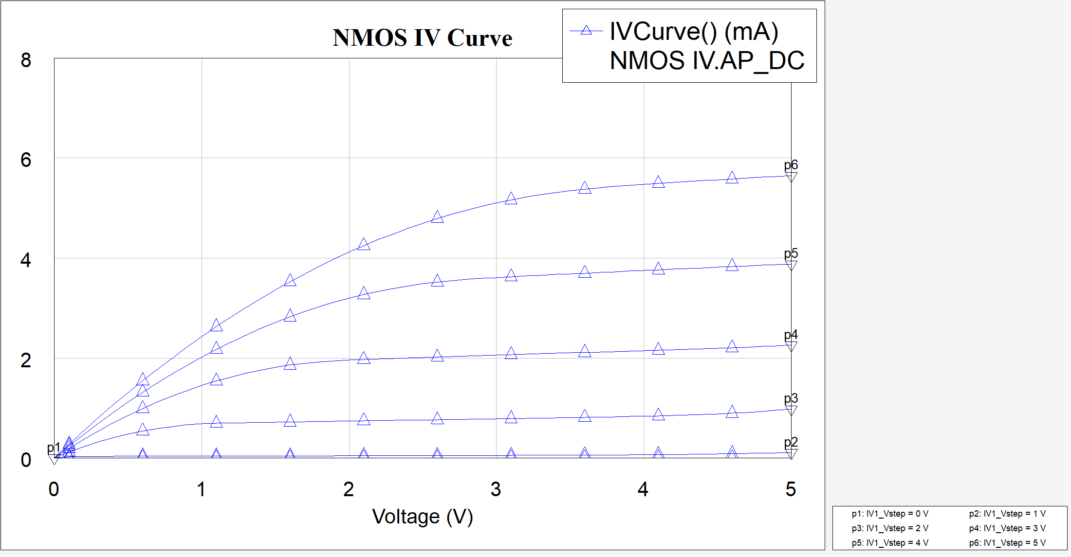
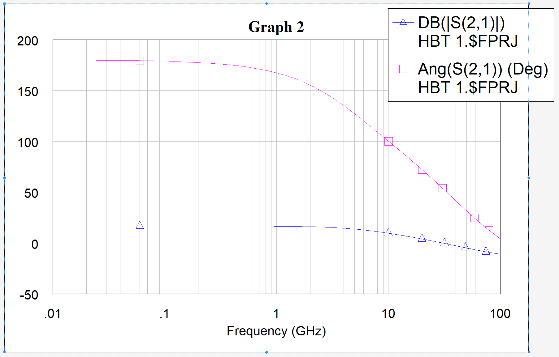
I began by characterizing a base NMOS schematic that was provided to use to understand its operating behavior. This included analyzing NMOS IV curves to estimate threshold voltage and studying HBT current gain and cutoff frequency to understand high-frequency limitations.
These steps helped me determine the proper biasing regions for linear operation, frequency-dependent gain behavior, and the practical limits of transistor performance at RF.
Noise Optimization and Device Scaling
A major focus of the project was minimizing noise figure, which is very important in RF front-end design. I looked at how bias current and device sizing affect noise performance and found optimal operating points for minimum noise.
I also scaled the number of emitter fingers to intentionally shift the optimum source impedance, observing how this impacted gain, input matching, and noise.
Input Matching and Emitter Degeneration
To improve input matching and stability, I added emitter degeneration inductance to see its effect on input impedance, noise figure, and the overall voltage gain.
While degeneration reduced gain, it significantly improved impedance matching and noise performance, which was teh first real trade-off I had to do as part of this project.
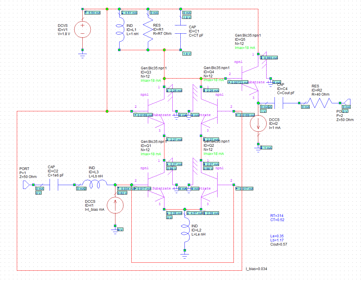
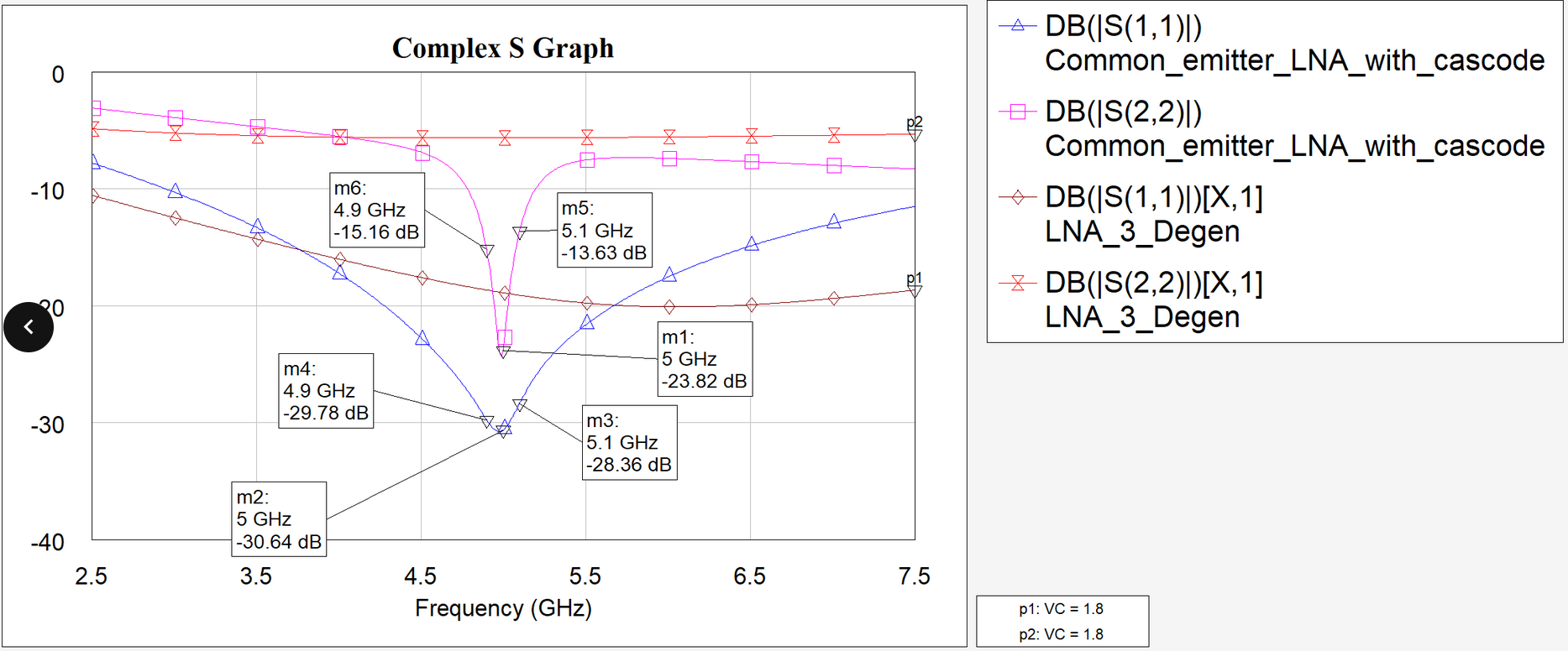
Low-Noise Amplifier Design
Using the insights from these earlier steps, I designed the final GHz-range low-noise amplifier, including input and output matching networks, biasing to remove noise, and attaching a frequency-selective tank circuits to improve its performance.
I compared a basic common-emitter amplifier against a this cascode topology, and noticed noticable improvements in gain and isolation while maintaining low noise.
Conclusion
By the end of the project, I was able to achieve high gain at GHz frequencies using the cascode LNA while significantly reducing noise figure through bias optimization and matching.
This project was quite different from other projects I had done. It gave me hands-on experience with RF amplifier design at the circuit level, something I had not worked with before. It's what really helped me understand how seemingly isolated things such as biasing, noise, matching, and frequency response are interconnected in a complete circuit like an LNA.